


This Industry Viewpoint was authored by Fady Masoud, Senior Director, Solutions Marketing at Nokia
The explosive growth of AI model training, inference and data movement across distributed, geographically distributed compute clusters is driving a sharp increase in east-west and data center interconnect traffic. Combined with increasing traffic from telecommunications providers expanding capacity in metro and long-haul links, this trend is placing new demands on optical pluggable design, pushing toward higher capacity and lower power-per-bit.
While 800G ZR and ZR+ coherent pluggables are already transforming the market, the next step is in sight: 1600G (1.6 Tb/s) ZR and ZR+ pluggables, offering even greater capacity in standardized, interoperable form factors.
Building a 1600G coherent pluggable small enough to fit within the OSFP1600 multi-source agreement is an engineering feat that further pushes many technological boundaries. Achieving this requires innovations across all aspects of coherent pluggable design, including advanced materials, modulators, digital signal processors (DSPs) and packaging.
Overcoming challenges in scaling to 1600G
To achieve 1600G in a pluggable, several key technology pillars must converge. It’s not just about making components smaller; it’s about making fundamental changes in how these building blocks are designed and how they operate.
- Operating at a very-high baud rate: To fit 1600G of capacity into a single wavelength, the symbol rate must be increased from the current ~140 GBaud (800G) to approximately 200 to 260 GBaud. This requires a radical redesign of the entire electro-optical path:
- Modulators: Traditional silicon photonics (SiPh) modulators have bandwidth limitations at these baud rates. The industry is shifting toward indium phosphide (InP) and new materials such as thin-film lithium niobate (TFLN), which offer higher bandwidth and lower drive voltages.
- Signal amplifiers and RF interconnect: The electrical amplifiers (driver and trans-impedance amplifier) must handle large volumes of bandwidth with minimal signal distortion and noise. Similarly, radio frequency (RF) interconnections between the DSP/ASIC and the analog electronics need to consider multiple factors, including RF crosstalk, reflections/echoes, positive/negative (P/N) balance/skew (latency differences between P/N voltages), and RF loss/bandwidth response.
- Power consumption: As DSPs grow more advanced and capable of processing 1600 Gb/s bit streams at higher baud rates, their overall power consumption rises, even as power consumption per bit decreases. This presents a significant challenge because host devices have a limited power budget for pluggable sockets.
- DSP demands: The DSP is the module’s brain. At 1600 Gb/s, the DSP must process twice the data in the same amount of time. Recovering high baud rate signals requires significant computational horsepower. Furthermore, when packaged in a compact coherent pluggable, such as OSFP1600, DSPs must operate within stringent space and thermal constraints, which limit many of their supported capabilities.
- Handling noise and impairments: As data rates climb, systems become increasingly sensitive to chromatic dispersion, equalization-enhanced phase noise (EEPN), optical noise, dispersion and nonlinearities, all of which can degrade signal quality and integrity if they exceed acceptable limits.
- Thermal and heat management: High-speed electronics and photonics produce heat that requires careful management within compact pluggable form factors.
These challenges are spurring a new wave of technological innovation across digital processing, materials use and modulation formats.
Enabling 1600G through technology innovation
Building on the experience gained from 800G, 1600G pluggables need major improvements to succeed.
- Advanced DSPs: 1600G coherent engines utilize 2 nm or 1.6 nm CMOS processes to supply the necessary processing power for high bit rates, symbol rates of 260 Gbaud and beyond, enhanced power efficiency and decreased latency. Key innovations, such as adaptive digital equalization and carrier phase estimation, are used to compensate for channel impairments like polarization mode dispersion and laser phase noise. Given the high bit rate and constraints on power consumption and size, DSPs must implement algorithms that provide sufficient power and sophistication to draw out the transmitted data from a signal warped by fiber impairments.
- Dual‑subcarrier designs: For extended-reach ZR+ applications, standards‑based implementations will use dual‑subcarrier architectures, splitting a 1600 Gb/s wavelength into two lower‑baud‑rate subcarriers to mitigate chromatic dispersion and EEPN. This method balances DSP complexity with laser requirements. For shorter‑reach 1600G ZR applications typically under 120 km, a single‑carrier approach similar to current 400G ZR and 800G ZR implementations will be used.
- Photonic materials and integration: Achieving 1600G ZR+ performance calls for more efficient photonic integration, likely using SiPh, InP and TFLN. These technologies support scaling to higher baud rates, enabling higher-order modulation, lower insertion loss and improved energy efficiency in compact designs. Both TFLN and InP modulators provide the wide bandwidth and linearity needed for high‑order coherent modulation, while keeping low drive voltage and reducing thermal sensitivity.
- Packaging and thermal design: These considerations remain key challenges for 1600G pluggables. The combination of higher baud rates, more capable DSPs and greater optical electrical integration leads to increased power density within the confined space and cooling limits of the pluggable. OSFP1600 is expected to be the primary form factor. It offers a large thermal envelope, making it best suited for early 1600G ZR+ deployments in switches, routers and DWDM platforms.
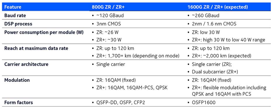
Table 1: Comparing 800G ZR/ZR+ and 1600G ZR/ZR+ coherent pluggables
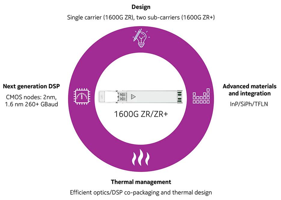
Figure 1: Design considerations for 1600G ZR/ZR+ Pluggables
Building a multi-vendor ecosystem
Multi-vendor interoperability remains a core part of the ZR and ZR+ value proposition. To support this, the Optical Internetworking Forum (OIF), representing both operators and vendors, launched the 1600ZR and the 1600ZR+ working groups in late 2023 and early 2024. These groups build on OIF’s 800G pluggable standardization efforts and aim to establish a standardized framework for 1600G. Their work focuses on defining parameters such as forward error correction, electrical interfaces and reach tiers to ensure that 1600G modules from different suppliers can interoperate and integrate into broader network architectures. Backward compatibility with 400G ZR and ZR+ as well as 800G ZR and ZR+ remains essential, supporting mixed-rate deployments and enabling networks to evolve without disruptive upgrades.
The journey to 1600G has already started
As the demand for higher-capacity networks grows, 1600G ZR and ZR+ modules, though not expected to be commercially available until mid- to late-2027, are already on the radar of network operators. Early planning is necessary given the lengthy design cycles of optical systems, routers and line cards, as well as the need to ensure interoperability across multi-vendor and mixed-rate ecosystems.
Successfully delivering 1600G coherent pluggables will require coordinated advancements across DSPs, photonics, packaging and thermal management, coupled with collaboration across the ecosystem to align on standards, interoperability, and deployment models. With AI traffic continuing to grow rapidly and network operators striving for greater efficiency and scalability, 1600G ZR and ZR+ promise to deliver capacity, flexibility, and openness to the optical industry.
About the Author
 Fady Masoud is a senior director for solutions marketing at Nokia focusing on next-generation intelligent coherent pluggable optics (ICE-X) and cloud /data center interconnect solutions. His area of expertise is the architecture and requirements of next-generation optical networking infrastructure. During his 30 years in the telecommunications industry, Fady has held various positions in the optical networking domain at Nortel, Ciena, Infinera, and now Nokia. He started as a hardware test engineer on the first OC-192 (10 Gb/s) systems and then was a systems and network engineer on optical transmission products, all combined with hands-on experience. Fady holds a bachelor’s degree in electrical engineering from Laval University (Quebec City, Canada) and a master’s degree in systems technology (software simulation of optical networks) from the Superior School of Technology (Montreal, Canada). He has written numerous industry and technical publications such as for the IEEE, as well as a book on next-generation optical networking, cloud networking, and data center interconnect, as well as on many other key topics.
If you haven't already, please take our Reader Survey! Just 3 questions to help us better understand who is reading Telecom Ramblings so we can serve you better!
Categories: Industry Viewpoint · Telecom Equipment
Discuss this Post